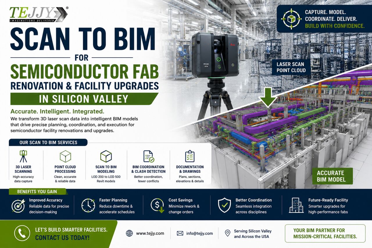
Our Scan to BIM workflow can help semiconductor owners, contractors, architects, and engineers with:
Existing-condition Revit modeling
Cleanroom and controlled-environment documentation
MEP and specialty system coordination
Process equipment spatial verification
Utility and infrastructure mapping
Renovation clash detection
As-built BIM development
Facility expansion and modernization planning
Capture existing conditions accurately and turn them into actionable BIM data for safer, better-coordinated fab upgrades.
Need accurate Scan to BIM modeling for a semiconductor project in Silicon Valley? Contact us today.
Contact Details -
Phone Number: 202-465-4830
Email Address: [email protected]
Website: https://www.tejjy.com/bim-s ...